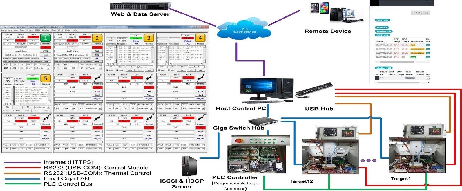
Testability Design

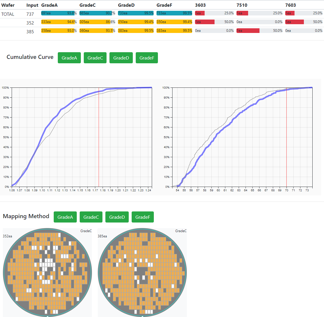
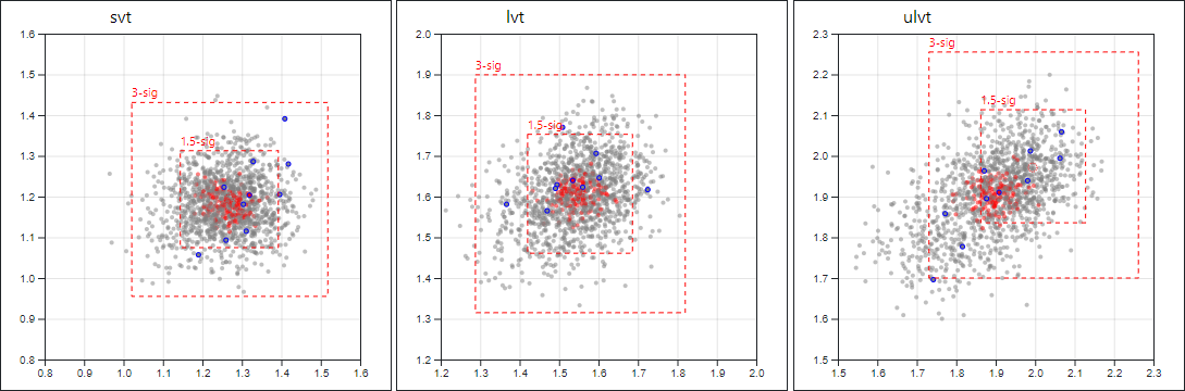
Result Analysis and Summary

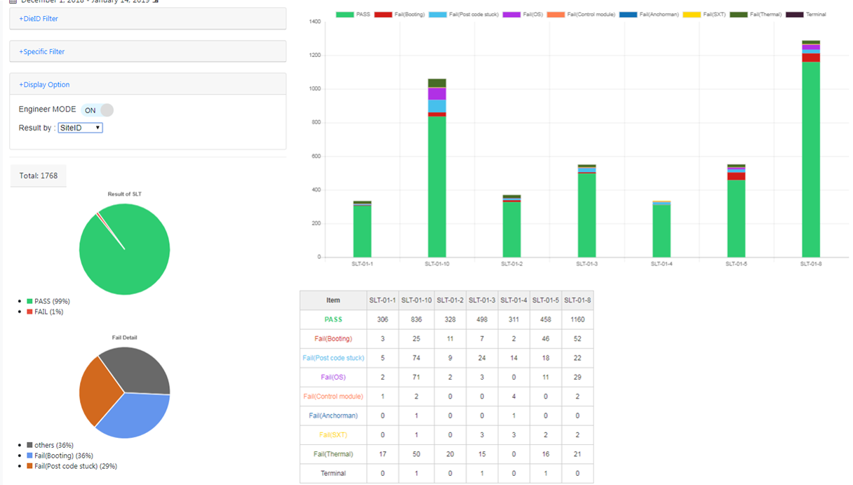
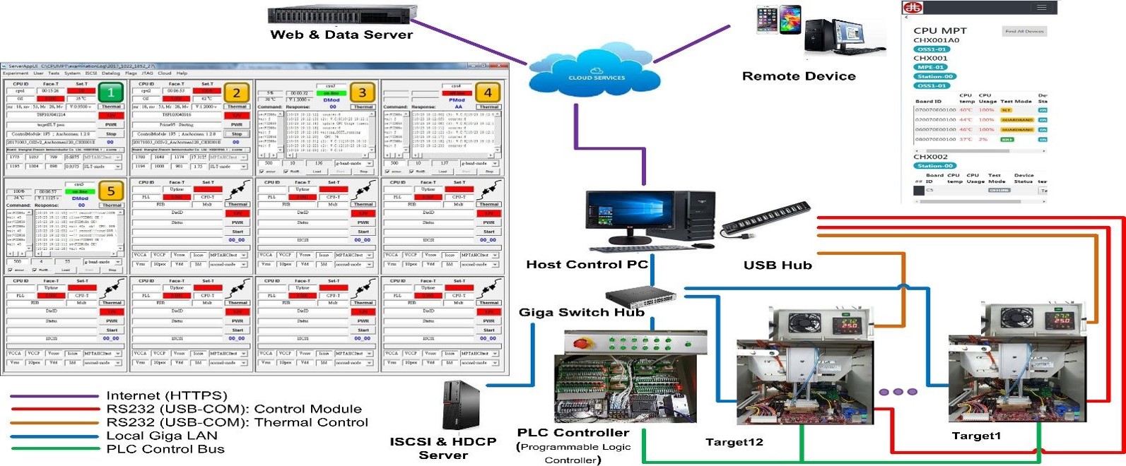
System Level Testing
Testability Design

Result Analysis and Summary

System Level Testing